🔧 From PCB to PCBA: A Deep Dive into Manufacturing & Assembly
The global electronics manufacturing market is projected to hit 💵 $797 billion by 2029, driven by innovations in 🔩 PCB fabrication, 🤖 PCBA assembly, and smarter design tools like 🛠️ Altium Designer and 💻 KiCad. But how do raw materials like ⚡ copper clad laminate transform into functional 🟢 94V0 circuit boards? Let’s break down the process.
1. 🎨 Design: Where Ideas Become Blueprints
- 📐 Schematic Capture: Tools like KiCad or Altium Designer turn concepts into schematics.
- 📊 PCB Stackups: Optimize layers for signal integrity in 🔌 multilayer circuit boards.
- 📋 BOM Creation: Learn 📦 how to make a BOM that aligns with 💰 PCB costing and component availability.
- 📏 Design Rules: Define gaps, trace widths, and 🕳️ via placements to avoid ❄️ cold solder joints.
2. 🏭 PCB Fabrication: Building the Foundation
- 🌡️ Materials: Choose 🔥 FR-4, 🌀 PTFE, or metal-core substrates based on thermal needs.
- 🖨️ Imaging & Etching: Laser direct imaging ensures precision for 🔍 high-density PCB circuits.
- ⚙️ Drilling & Plating: Create 🕳️ vias and through-holes for 🔘 dual inline packages (DIP).
- 🎨 Solder Mask & Silkscreen: Apply green or custom 🌈 PCB colors for durability and labeling.
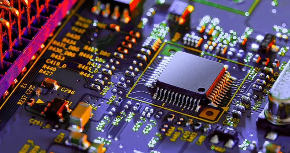
3. 🤖 PCBA Assembly: Components Meet the Board
- ⚡ SMT Process: Machines place 🔳 BGA and 🔘 chip-on-board components at lightning speed.
- 🔩 Through-Hole Assembly: Secure 🔌 DIP packages with 🌱 lead-free solder for RoHS compliance.
- 🔥 Reflow vs. 🌊 Wave Soldering: Balance speed (SMT) vs. reliability (through-hole).
4. ✅ Testing & Quality Control
- 📸 AOI & X-Ray: Detect ❄️ cold solder joints and misalignments in 🔌 multilayer PCBs.
- 📜 IPC Class Standards: Ensure compliance for medical, automotive, or consumer electronics.
- 🛠️ Functional Testing: Validate performance under extreme conditions (e.g., 🟢 94V-0 circuit boards).
5. 💰 Cost Drivers in PCB Production
- 📦 Material Choices: ⚡ Copper clad laminate grades impact 💲 PCB prices.
- 📚 Layer Count: 🔌 Multilayer circuit boards cost more but save space.
- ✨ Surface Finish: HASL vs. ENIG for 🏢 PCB assembly services.
📱 Social Media Teaser:
“Did you know a single ❄️ cold solder joint can derail your 🔧 PCBA manufacturing? Discover how 🛠️ Altium, ⚡ SMT lines, and 📜 IPC Class standards ensure flawless electronics!”
🔑 Key Takeaways:
- Use 💻 KiCad or 🛠️ Altium Designer for error-free schematics and 📊 PCB stackups.
- Prioritize 📜 IPC Class compliance to avoid field failures.
- Optimize 💰 PCB costing by balancing 🔥 FR-4 and 🌀 high-frequency materials.
[🆚 Image: Side-by-side comparison of PCB vs. PCBA]
Caption: PCB (bare board) 🆚 PCBA (assembled with components).
By mastering these steps, you’ll streamline 🏭 PCB fabrication and assembly, reduce 💲 PCB prices, and deliver robust 🔩 printed circuit board assemblies—whether for 🔘 dual inline packages or cutting-edge 🔳 BGA designs.