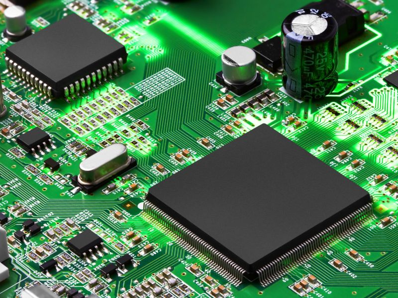
Introduction to PCBA
PCBA (Printed Circuit Board Assembly) is the process of mounting electronic components onto a PCB (Printed Circuit Board) to create functional electronic devices. This guide explores the entire PCBA process, from design to final assembly, including materials and manufacturing techniques.

PCBA Assembly Process

The PCBA process involves several key steps:

- Design & Preparation: Using software like Altium Designer or KiCad, designers create a PCB layout that outlines component placement and circuit paths. This design is then printed onto a copper-clad laminate using specialized equipment.
- Component Sourcing: High-quality components such as resistors, capacitors, and ICs are sourced based on the BOM (Bill of Materials) specifications.
- PCB Fabrication: The PCB is fabricated through a series of steps including etching, drilling, and plating to create the desired circuit pattern.
- Solder Paste Application: Solder paste is applied to the PCB pads using a stencil to ensure precise placement.
- Component Placement: Automated pick-and-place machines position SMT components onto the PCB with high accuracy.
- Soldering: Components are soldered using either reflow soldering for SMT components or wave soldering for THT components.
- Inspection & Testing: Automated Optical Inspection (AOI) and electrical tests ensure quality and functionality
- Final Assembly & Packaging: The PCB is integrated into the final product, which may include adding connectors or enclosures.
Types of PCBA Assembly

PCBA involves different assembly types tailored to specific applications:
| Assembly Type | Features | Applications |
|---|---|---|
| Single-Sided Assembly | Components mounted on one side; cost-effective for simple designs. | Remote controls, battery boards |
| Double-Sided Assembly | Components on both sides; supports higher density and complexity. | Communication devices, computers |
| Through-Hole Technology (THT) | Components’ leads pass through PCB holes for strong mechanical bonds. | Industrial equipment, military-grade electronics |
| Surface Mount Technology (SMT) | Compact and lightweight; components mounted directly onto the PCB surface. | Smartphones, IoT devices |
| Mixed Assembly | Combines SMT and THT for specific performance needs. | High-performance electronics |
PCB Materials and Manufacturing Insights
Manufacturing trends include advancements in automation, sustainable practices, and miniaturization techniques.
PCB materials play a crucial role in determining performance and durability:
- FR-4: A widely used fiberglass-reinforced epoxy laminate offering excellent insulation and mechanical strength.
- Copper-Clad Laminates: Provide conductive layers essential for signal transmission.
- Polyimide: Used in high-temperature or flexible PCB applications.
- Metal Substrates (Aluminum/Copper): Ideal for heat dissipation in power electronics.
Emerging materials like graphene and nanomaterials are also gaining traction for advanced applications such as 5G networks and IoT devices.
Soldering Techniques in PCBA

Soldering ensures electrical connections between components and the PCB:
- Reflow Soldering: Common in SMT processes for precise bonding.
- Wave Soldering: Used primarily for THT assemblies.
- Lead-Free Soldering: Eco-friendly alternatives compliant with RoHS regulations.
Advanced methods like ultrasonic welding or laser soldering are used for specialized applications requiring high precision.

Future Trends in PCBA Manufacturing
By 2025, innovations in PCB manufacturing are shaping the industry:
- AI-Powered Automation: Enhances design optimization and defect detection during assembly.
- Sustainable Practices: Lead-free soldering and recyclable substrates reduce environmental impact.
- 3D Printing of PCBs: Enables rapid prototyping and complex designs.
- Miniaturization & Integration: Smaller devices demand compact multilayer circuit boards with integrated components.